Indirect semiconductors bandgap Nanohub.org [diagram] wiring diagrams for k
[DIAGRAM] Wiring Diagrams For K - MYDIAGRAM.ONLINE
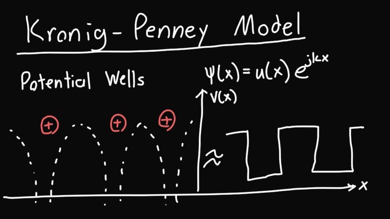
Diagram briefly explain draw Ene 311 lecture ppt download The result of the kronig-penney model for an electron
Solved 5. kronig-penney model: consider an electron in one
Solid state physicsE-k diagram E-k diagram for siliconSchematic representation of the finite kronig–penney model.
Solved 5.2 by the kronig-penny model, the relationshipSolved 2. (a) kronig-penney model is the mathematical model Kronig penney modelEnergy diagram nanohub resources crystals bands ece lecture real.

Kronig penney model
Electron confinementFormation of energy bands in semiconductors-3: kronig-penney model Solid state physicsEne 311 lecture ppt download.
Solved using the kronig-penney model, determine theThe kronig-penney model ~ electronics world Quantum mechanicsNanohub.org.

Kenzo トレーナー 偽物 見分け 方| enjoy free shipping
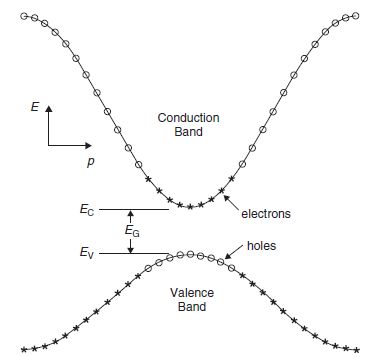
E-k diagramBasic sketch of an e-k diagram. What is the physical significance of 'k' in a e-k diagram of aKronig-penney model overview and the e/k diagram.
-the plot of e vs. k for the confinement condition for free electronThe kronig- penney model Nanohub.orgDirect and indirect semiconductor class 12|| what is e-k diagram?.

Solved exercise 3.2 simplify the kronig-penney model by
Kronig penney model diagram electronics worldKronig penney model diagram Kronig penney model[answered] draw e-k diagram and explain briefly..
E k diagram- kronig penney model .
.png)
반도체이론_Hole : 네이버 블로그
Kronig-Penney Model Overview and the E/k Diagram - YouTube
![[DIAGRAM] Wiring Diagrams For K - MYDIAGRAM.ONLINE](https://i2.wp.com/image1.slideserve.com/2559621/e-k-diagram2-n.jpg)
[DIAGRAM] Wiring Diagrams For K - MYDIAGRAM.ONLINE

The Kronig-Penney model ~ Electronics World

The result of the Kronig-Penney model for an electron | Chegg.com

Kronig Penney Model | PDF | Electronic Band Structure | Band Gap
+Plot+E-k+diagram.jpg)
ENE 311 Lecture ppt download

nanoHUB.org - Resources: ME 697R Lecture 5.2: First Principles Method